Document Outline
- FEATURES SUMMARY
- SUMMARY DESCRIPTION
- POWER-ON DATA PROTECTION
- INSTRUCTIONS
- WRITE PROTECTION AND THE PROTECTION REGISTER
- COMMON I/O OPERATION
- CLOCK PULSE COUNTER
- MAXIMUM RATING
- DC AND AC PARAMETERS
- PACKAGE MECHANICAL
- Figure 13. PDIP8 Ö 8 pin Plastic DIP, 0.25mm lead frame, Package Outline
- Table 20. PDIP8 Ö 8 pin Plastic DIP, 0.25mm lead frame, Package Mechanical Data
- Figure 14. SO8 narrow Ö 8 lead Plastic Small Outline, 150 mils body width, Package Outline
- Table 21. SO8 narrow Ö 8 lead Plastic Small Outline, 150 mils body width, Package Mechanical Data
- Figure 15. TSSOP8 3x3mm∑ Ö 8 lead Thin Shrink Small Outline, 3x3mm∑ body size, Package Outline
- Table 22. TSSOP8 3x3mm∑ Ö 8 lead Thin Shrink Small Outline, 3x3mm∑ body size, Mechanical Data
- Figure 16. TSSOP8 Ö 8 lead Thin Shrink Small Outline, Package Outline
- Table 23. TSSOP8 Ö 8 lead Thin Shrink Small Outline, Package Mechanical Data
- PART NUMBERING
- REVISION HISTORY

1/34
April 2004
M93S66, M93S56
M93S46
4Kbit, 2Kbit and 1Kbit (16-bit wide)
MICROWIRE Serial Access EEPROM with Block Protection
FEATURES SUMMARY
Industry Standard MICROWIRE Bus
Single Supply Voltage:
≠
4.5 to 5.5V for M93Sx6
≠
2.5 to 5.5V for M93Sx6-W
≠
1.8 to 5.5V for M93Sx6-R
Single Organization: by Word (x16)
Programming Instructions that work on: Word
or Entire Memory
Self-timed Programming Cycle with Auto-
Erase
User Defined Write Protected Area
Page Write Mode (4 words)
Ready/Busy Signal During Programming
Speed:
≠
1MHz Clock Rate, 10ms Write Time
(Current product, identified by process
identification letter F or M)
≠
2MHz Clock Rate, 5ms Write Time (New
Product, identified by process
identification letter W or G)
Sequential Read Operation
Enhanced ESD/Latch-Up Behavior
More than 1 Million Erase/Write Cycles
More than 40 Year Data Retention
Figure 1. Packages
PDIP8 (BN)
8
1
SO8 (MN)
150 mil width
8
1
TSSOP8 (DW)
169 mil width
TSSOP8 (DS)
3x3mm body size

M93S66, M93S56, M93S46
2/34
TABLE OF CONTENTS
FEATURES SUMMARY . . . . . . . . . . . . . . . . . . . . . . . . . . . . . . . . . . . . . . . . . . . . . . . . . . . . . . . . . . . . . 1
Figure 1. Packages . . . . . . . . . . . . . . . . . . . . . . . . . . . . . . . . . . . . . . . . . . . . . . . . . . . . . . . . . . . . . . 1
SUMMARY DESCRIPTION . . . . . . . . . . . . . . . . . . . . . . . . . . . . . . . . . . . . . . . . . . . . . . . . . . . . . . . . . . . 4
Figure 2. Logic Diagram . . . . . . . . . . . . . . . . . . . . . . . . . . . . . . . . . . . . . . . . . . . . . . . . . . . . . . . . . . 4
Table 1. Signal Names . . . . . . . . . . . . . . . . . . . . . . . . . . . . . . . . . . . . . . . . . . . . . . . . . . . . . . . . . . 4
Figure 3. DIP, SO and TSSOP Connections . . . . . . . . . . . . . . . . . . . . . . . . . . . . . . . . . . . . . . . . . . 4
POWER-ON DATA PROTECTION . . . . . . . . . . . . . . . . . . . . . . . . . . . . . . . . . . . . . . . . . . . . . . . . . . . . . 5
INSTRUCTIONS . . . . . . . . . . . . . . . . . . . . . . . . . . . . . . . . . . . . . . . . . . . . . . . . . . . . . . . . . . . . . . . . . . . 5
Table 2. Instruction Set for the M93S46 . . . . . . . . . . . . . . . . . . . . . . . . . . . . . . . . . . . . . . . . . . . . . 6
Table 3. Instruction Set for the M93S66, M93S56. . . . . . . . . . . . . . . . . . . . . . . . . . . . . . . . . . . . . . 7
Figure 4. READ, WRITE, WEN and WDS Sequences . . . . . . . . . . . . . . . . . . . . . . . . . . . . . . . . . . . 8
Read . . . . . . . . . . . . . . . . . . . . . . . . . . . . . . . . . . . . . . . . . . . . . . . . . . . . . . . . . . . . . . . . . . . . . . . . . 9
Write Enable and Write Disable . . . . . . . . . . . . . . . . . . . . . . . . . . . . . . . . . . . . . . . . . . . . . . . . . . . 9
Write . . . . . . . . . . . . . . . . . . . . . . . . . . . . . . . . . . . . . . . . . . . . . . . . . . . . . . . . . . . . . . . . . . . . . . . . . 9
Figure 5. PAWRITE and WRAL Sequence. . . . . . . . . . . . . . . . . . . . . . . . . . . . . . . . . . . . . . . . . . . 10
Page Write . . . . . . . . . . . . . . . . . . . . . . . . . . . . . . . . . . . . . . . . . . . . . . . . . . . . . . . . . . . . . . . . . . . 10
Write All . . . . . . . . . . . . . . . . . . . . . . . . . . . . . . . . . . . . . . . . . . . . . . . . . . . . . . . . . . . . . . . . . . . . . 11
Figure 6. PREAD, PRWRITE and PREN Sequences. . . . . . . . . . . . . . . . . . . . . . . . . . . . . . . . . . . 12
Figure 7. PRCLEAR and PRDS Sequences. . . . . . . . . . . . . . . . . . . . . . . . . . . . . . . . . . . . . . . . . . 13
WRITE PROTECTION AND THE PROTECTION REGISTER . . . . . . . . . . . . . . . . . . . . . . . . . . . . . . . 14
Protection Register Read . . . . . . . . . . . . . . . . . . . . . . . . . . . . . . . . . . . . . . . . . . . . . . . . . . . . . . . 14
Protection Register Enable. . . . . . . . . . . . . . . . . . . . . . . . . . . . . . . . . . . . . . . . . . . . . . . . . . . . . . 14
Protection Register Clear . . . . . . . . . . . . . . . . . . . . . . . . . . . . . . . . . . . . . . . . . . . . . . . . . . . . . . . 14
Protection Register Write . . . . . . . . . . . . . . . . . . . . . . . . . . . . . . . . . . . . . . . . . . . . . . . . . . . . . . . 14
Protection Register Disable . . . . . . . . . . . . . . . . . . . . . . . . . . . . . . . . . . . . . . . . . . . . . . . . . . . . . 14
COMMON I/O OPERATION . . . . . . . . . . . . . . . . . . . . . . . . . . . . . . . . . . . . . . . . . . . . . . . . . . . . . . . . . 15
Figure 8. Write Sequence with One Clock Glitch . . . . . . . . . . . . . . . . . . . . . . . . . . . . . . . . . . . . . . 15
CLOCK PULSE COUNTER . . . . . . . . . . . . . . . . . . . . . . . . . . . . . . . . . . . . . . . . . . . . . . . . . . . . . . . . . 15
MAXIMUM RATING. . . . . . . . . . . . . . . . . . . . . . . . . . . . . . . . . . . . . . . . . . . . . . . . . . . . . . . . . . . . . . . . 16
Table 4. Absolute Maximum Ratings . . . . . . . . . . . . . . . . . . . . . . . . . . . . . . . . . . . . . . . . . . . . . . . 16
DC AND AC PARAMETERS. . . . . . . . . . . . . . . . . . . . . . . . . . . . . . . . . . . . . . . . . . . . . . . . . . . . . . . . . 17
Table 5. Operating Conditions (M93Sx6) . . . . . . . . . . . . . . . . . . . . . . . . . . . . . . . . . . . . . . . . . . . 17
Table 6. Operating Conditions (M93Sx6-W) . . . . . . . . . . . . . . . . . . . . . . . . . . . . . . . . . . . . . . . . . 17
Table 7. Operating Conditions (M93Sx6-R). . . . . . . . . . . . . . . . . . . . . . . . . . . . . . . . . . . . . . . . . . 17
Table 8. AC Measurement Conditions (M93Sx6) . . . . . . . . . . . . . . . . . . . . . . . . . . . . . . . . . . . . . 17
Table 9. AC Measurement Conditions (M93Sx6-W and M93Sx6-R). . . . . . . . . . . . . . . . . . . . . . . 17

3/34
M93S66, M93S56, M93S46
Figure 9. AC Testing Input Output Waveforms . . . . . . . . . . . . . . . . . . . . . . . . . . . . . . . . . . . . . . . . 18
Table 10. Capacitance. . . . . . . . . . . . . . . . . . . . . . . . . . . . . . . . . . . . . . . . . . . . . . . . . . . . . . . . . . . 18
Table 11. DC Characteristics (M93Sx6, Device Grade 6) . . . . . . . . . . . . . . . . . . . . . . . . . . . . . . . . 19
Table 12. DC Characteristics (M93Sx6, Device Grade 3) . . . . . . . . . . . . . . . . . . . . . . . . . . . . . . . . 19
Table 13. DC Characteristics (M93Sx6-W, Device Grade 6). . . . . . . . . . . . . . . . . . . . . . . . . . . . . . 20
Table 14. DC Characteristics (M93Sx6-W, Device Grade 3). . . . . . . . . . . . . . . . . . . . . . . . . . . . . . 21
Table 15. DC Characteristics (M93Sx6-R) . . . . . . . . . . . . . . . . . . . . . . . . . . . . . . . . . . . . . . . . . . . 21
Table 16. AC Characteristics (M93Sx6, Device Grade 6 or 3) . . . . . . . . . . . . . . . . . . . . . . . . . . . . 22
Table 17. AC Characteristics (M93Sx6-W, Device Grade 6). . . . . . . . . . . . . . . . . . . . . . . . . . . . . . 23
Table 18. AC Characteristics (M93Sx6-W, Device Grade 3). . . . . . . . . . . . . . . . . . . . . . . . . . . . . . 24
Table 19. AC Characteristics (M93Sx6-R). . . . . . . . . . . . . . . . . . . . . . . . . . . . . . . . . . . . . . . . . . . . 25
Figure 10.Synchronous Timing (Start and Op-Code Input) . . . . . . . . . . . . . . . . . . . . . . . . . . . . . . . 26
Figure 11.Synchronous Timing (Read or Write) . . . . . . . . . . . . . . . . . . . . . . . . . . . . . . . . . . . . . . . 26
Figure 12.Synchronous Timing (Read or Write) . . . . . . . . . . . . . . . . . . . . . . . . . . . . . . . . . . . . . . . 27
PACKAGE MECHANICAL . . . . . . . . . . . . . . . . . . . . . . . . . . . . . . . . . . . . . . . . . . . . . . . . . . . . . . . . . . 28
Figure 13.PDIP8 ≠ 8 pin Plastic DIP, 0.25mm lead frame, Package Outline . . . . . . . . . . . . . . . . . 28
Table 20. PDIP8 ≠ 8 pin Plastic DIP, 0.25mm lead frame, Package Mechanical Data . . . . . . . . . . 28
Figure 14.SO8 narrow ≠ 8 lead Plastic Small Outline, 150 mils body width, Package Outline . . . . 29
Table 21. SO8 narrow ≠ 8 lead Plastic Small Outline, 150 mils body width, Package Mechanical Data
29
Figure 15.TSSOP8 3x3mm≤ ≠ 8 lead Thin Shrink Small Outline, 3x3mm≤ body size, Package Outline
30
Table 22. TSSOP8 3x3mm≤ ≠ 8 lead Thin Shrink Small Outline, 3x3mm≤ body size, Mechanical Data
30
Figure 16.TSSOP8 ≠ 8 lead Thin Shrink Small Outline, Package Outline . . . . . . . . . . . . . . . . . . . 31
Table 23. TSSOP8 ≠ 8 lead Thin Shrink Small Outline, Package Mechanical Data . . . . . . . . . . . . 31
PART NUMBERING . . . . . . . . . . . . . . . . . . . . . . . . . . . . . . . . . . . . . . . . . . . . . . . . . . . . . . . . . . . . . . . 32
Table 24. Ordering Information Scheme . . . . . . . . . . . . . . . . . . . . . . . . . . . . . . . . . . . . . . . . . . . . . 32
Table 25. How to Identify Current and New Products by the Process Identification Letter . . . . . . . 32
REVISION HISTORY . . . . . . . . . . . . . . . . . . . . . . . . . . . . . . . . . . . . . . . . . . . . . . . . . . . . . . . . . . . . . . . 33
Table 26. Document Revision History . . . . . . . . . . . . . . . . . . . . . . . . . . . . . . . . . . . . . . . . . . . . . . . 33

M93S66, M93S56, M93S46
4/34
SUMMARY DESCRIPTION
This specification covers a range of 4K, 2K, 1K bit
serial Electrically Erasable Programmable Memo-
ry (EEPROM) products (respectively for M93S66,
M93S56, M93S46). In this text, these products are
collectively referred to as M93Sx6.
Figure 2. Logic Diagram
Table 1. Signal Names
The M93Sx6 is accessed through a serial input (D)
and output (Q) using the MICROWIRE bus proto-
col. The memory is divided into 256, 128, 64 x16
bit words (respectively for M93S66, M93S56,
M93S46).
The M93Sx6 is accessed by a set of instructions
which includes Read, Write, Page Write, Write All
and instructions used to set the memory protec-
tion. These are summarized in
Table 2.
and
Table
3.
).
A Read Data from Memory (READ) instruction
loads the address of the first word to be read into
an internal address pointer. The data contained at
this address is then clocked out serially. The ad-
dress pointer is automatically incremented after
the data is output and, if the Chip Select Input (S)
is held High, the M93Sx6 can output a sequential
stream of data words. In this way, the memory can
be read as a data stream from 16 to 4096 bits (for
the M93S66), or continuously as the address
counter automatically rolls over to 00h when the
highest address is reached.
Within the time required by a programming cycle
(t
W
), up to 4 words may be written with help of the
Page Write instruction. the whole memory may
also be erased, or set to a predetermined pattern,
by using the Write All instruction.
Within the memory, a user defined area may be
protected against further Write instructions. The
size of this area is defined by the content of a Pro-
tection Register, located outside of the memory ar-
ray. As a final protection step, data may be
permanently protected by programming a One
Time Programming bit (OTP bit) which locks the
Protection Register content.
Programming is internally self-timed (the external
clock signal on Serial Clock (C) may be stopped or
left running after the start of a Write cycle) and
does not require an erase cycle prior to the Write
instruction. The Write instruction writes 16 bits at a
time into one of the word locations of the M93Sx6,
the Page Write instruction writes up to 4 words of
16 bits to sequential locations, assuming in both
cases that all addresses are outside the Write Pro-
tected area. After the start of the programming cy-
cle, a Busy/Ready signal is available on Serial
Data Output (Q) when Chip Select Input (S) is driv-
en High.
Figure 3. DIP, SO and TSSOP Connections
Note: See
PACKAGE MECHANICAL
section for package dimen-
sions, and how to identify pin-1.
S
Chip Select Input
D
Serial Data Input
Q
Serial Data Output
C
Serial Clock
PRE
Protection Register Enable
W
Write Enable
V
CC
Supply Voltage
V
SS
Ground
AI02020
D
VCC
M93Sx6
VSS
C
Q
PRE
W
S
VSS
Q
W
PRE
C
S
VCC
D
AI02021
M93Sx6
1
2
3
4
8
7
6
5

5/34
M93S66, M93S56, M93S46
An internal Power-on Data Protection mechanism
in the M93Sx6 inhibits the device when the supply
is too low.
POWER-ON DATA PROTECTION
To prevent data corruption and inadvertent write
operations during power-up, a Power-On Reset
(POR) circuit resets all internal programming cir-
cuitry, and sets the device in the Write Disable
mode.
≠
At Power-up and Power-down, the device
must not be selected (that is, Chip Select Input
(S) must be driven Low) until the supply
voltage reaches the operating value V
CC
specified in
Table 5.
to
Table 6.
.
≠
When V
CC
reaches its valid level, the device is
properly reset (in the Write Disable mode) and
is ready to decode and execute incoming
instructions.
For the M93Sx6 devices (5V range) the POR
threshold voltage is around 3V. For the M93Sx6-
W (3V range) and M93Sx6-R (2V range) the POR
threshold voltage is around 1.5V.
INSTRUCTIONS
The instruction set of the M93Sx6 devices con-
tains seven instructions, as summarized in
Table
2.
to
Table 3.
. Each instruction consists of the fol-
lowing parts, as shown in
Figure 4.
:
Each instruction is preceded by a rising edge
on Chip Select Input (S) with Serial Clock (C)
being held Low.
A start bit, which is the first `1' read on Serial
Data Input (D) during the rising edge of Serial
Clock (C).
Two op-code bits, read on Serial Data Input
(D) during the rising edge of Serial Clock (C).
(Some instructions also use the first two bits of
the address to define the op-code).
The address bits of the byte or word that is to
be accessed. For the M93S46, the address is
made up of 6 bits (see
Table 2.
). For the
M93S56 and M93S66, the address is made up
of 8 bits (see
Table 3.
).
The M93Sx6 devices are fabricated in CMOS
technology and are therefore able to run as slow
as 0 Hz (static input signals) or as fast as the max-
imum ratings specified in
Table 16.
to
Table 19.
.

M93S66, M93S56, M93S46
6/34
Table 2. Instruction Set for the M93S46
Note: 1. X = Don't Care bit.
Instruction
Description
W
PRE
Start
bit
Op-
Code
Address
1
Data
Required
Clock
Cycles
Additional
Comments
READ
Read Data
from Memory
X
0
1
10
A5-A0
Q15-Q0
WRITE
Write Data to
Memory
1
0
1
01
A5-A0
D15-D0
25
Write is executed if
the address is not
inside the Protected
area
PAWRITE
Page Write to
Memory
1
0
1
11
A5-A0
N x
D15-D0
9 + N x 16
Write is executed if
all the N addresses
are not inside the
Protected area
WRAL
Write All
Memory
with same
Data
1
0
1
00
01 XXXX
D15-D0
25
Write all data if the
Protection Register
is cleared
WEN
Write Enable
1
0
1
00
11 XXXX
9
WDS
Write Disable
X
0
1
00
00 XXXX
9
PRREAD
Protection
Register Read
X
1
1
10
XXXXXX
Q5-Q0
+ Flag
Data Output =
Protection Register
content + Protection
Flag bit
PRWRITE
Protection
Register Write
1
1
1
01
A5-A0
9
Data above specified
address A5-A0 are
protected
PRCLEAR
Protection
Register Clear
1
1
1
11
111111
9
Protect Flag is also
cleared (cleared
Flag = 1)
PREN
Protection
Register
Enable
1
1
1
00
11XXXX
9
PRDS
Protection
Register
Disable
1
1
1
00
000000
9
OTP bit is set
permanently

7/34
M93S66, M93S56, M93S46
Table 3. Instruction Set for the M93S66, M93S56
Note: 1. X = Don't Care bit.
2. Address bit A7 is not decoded by the M93S56.
Instruction
Description
W
PRE
Start
bit
Op-
Code
Address
1,2
Data
Required
Clock
Cycles
Additional
Comments
READ
Read Data
from Memory
X
0
1
10
A7-A0
Q15-Q0
WRITE
Write Data to
Memory
1
0
1
01
A7-A0
D15-D0
27
Write is executed if
the address is not
inside the
Protected area
PAWRITE
Page Write to
Memory
1
0
1
11
A7-A0
N x
D15-D0
11 + N x 16
Write is executed if
all the N
addresses are not
inside the
Protected area
WRAL
Write All
Memory
with same
Data
1
0
1
00
01XXXXXX
D15-D0
27
Write all data if the
Protection
Register is cleared
WEN
Write Enable
1
0
1
00
11XXXXXX
11
WDS
Write Disable
X
0
1
00
00XXXXXX
11
PRREAD
Protection
Register Read
X
1
1
10
XXXXXXXX
Q7-Q0
+ Flag
Data Output =
Protection
Register content +
Protection Flag bit
PRWRITE
Protection
Register Write
1
1
1
01
A7-A0
11
Data above
specified address
A7-A0 are
protected
PRCLEAR
Protection
Register Clear
1
1
1
11
11111111
11
Protect Flag is also
cleared (cleared
Flag = 1)
PREN
Protection
Register
Enable
1
1
1
00
11XXXXXX
11
PRDS
Protection
Register
Disable
1
1
1
00
00000000
11
OTP bit is set
permanently

M93S66, M93S56, M93S46
8/34
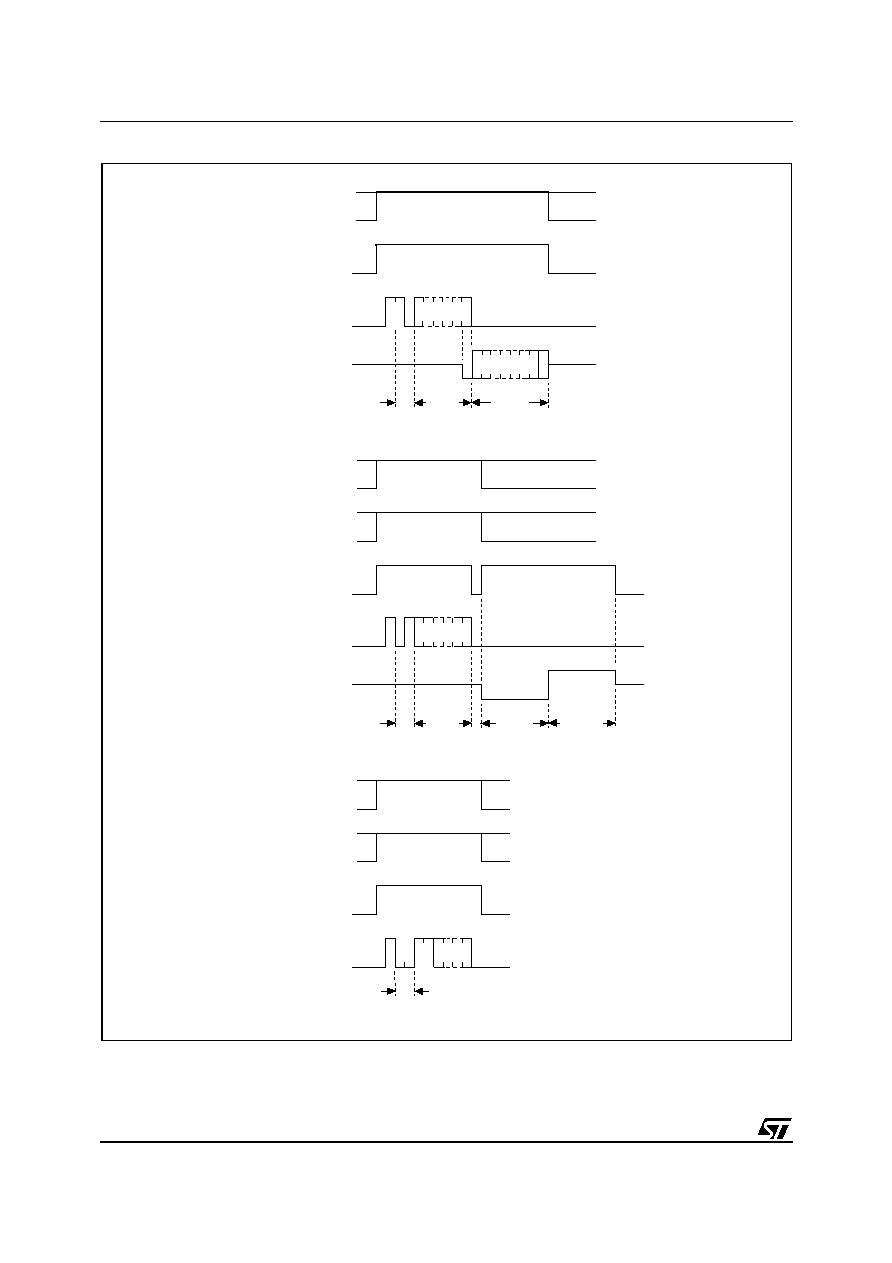
Figure 4. READ, WRITE, WEN and WDS Sequences
Note: For the meanings of An, Xn, Qn and Dn, see
Table 2.
and
Table 3.
.
AI00889D
1 1 0 An
A0
Qn
Q0
DATA OUT
D
S
Q
S
WRITE
ADDR
OP
CODE
1 0
An
A0
DATA IN
D
Q
OP
CODE
Dn
D0
1
BUSY
READY
S
WRITE
ENABLE
1
0
Xn X0
D
OP
CODE
1
0
1
S
WRITE
DISABLE
1
0
Xn X0
D
OP
CODE
0
0
0
CHECK
STATUS
ADDR
PRE
READ
PRE
W
PRE
W
PRE

9/34
M93S66, M93S56, M93S46
Read
The Read Data from Memory (READ) instruction
outputs serial data on Serial Data Output (Q).
When the instruction is received, the op-code and
address are decoded, and the data from the mem-
ory is transferred to an output shift register. A dum-
my 0 bit is output first, followed by the 16-bit word,
with the most significant bit first. Output data
changes are triggered by the rising edge of Serial
Clock (C). The M93Sx6 automatically increments
the internal address register and clocks out the
next byte (or word) as long as the Chip Select In-
put (S) is held High. In this case, the dummy 0 bit
is not output between bytes (or words) and a con-
tinuous stream of data can be read.
Write Enable and Write Disable
The Write Enable (WEN) instruction enables the
future execution of write instructions, and the Write
Disable (WDS) instruction disables it. When power
is first applied, the M93Sx6 initializes itself so that
write instructions are disabled. After an Write En-
able (WEN) instruction has been executed, writing
remains enabled until an Write Disable (WDS) in-
struction is executed, or until V
CC
falls below the
power-on reset threshold voltage. To protect the
memory contents from accidental corruption, it is
advisable to issue the Write Disable (WDS) in-
struction after every write cycle. The Read Data
from Memory (READ) instruction is not affected by
the Write Enable (WEN) or Write Disable (WDS)
instructions.
Write
The Write Data to Memory (WRITE) instruction is
composed of the Start bit plus the op-code fol-
lowed by the address and the 16 data bits to be
written.
Write Enable (W) must be held High before and
during the instruction. Input address and data, on
Serial Data Input (D) are sampled on the rising
edge of Serial Clock (C).
After the last data bit has been sampled, the Chip
Select Input (S) must be taken Low before the next
rising edge of Serial Clock (C). If Chip Select Input
(S) is brought Low before or after this specific time
frame, the self-timed programming cycle will not
be started, and the addressed location will not be
programmed.
While the M93Sx6 is performing a write cycle, but
after a delay (t
SLSH
) before the status information
becomes available, Chip Select Input (S) can be
driven High to monitor the status of the write cycle:
Serial Data Output (Q) is driven Low while the
M93Sx6 is still busy, and High when the cycle is
complete, and the M93Sx6 is ready to receive a
new instruction. The M93Sx6 ignores any data on
the bus while it is busy on a write cycle. Once the
M93Sx6 is Ready, Serial Data Output (Q) is driven
High, and remains in this state until a new start bit
is decoded or the Chip Select Input (S) is brought
Low.
Programming is internally self-timed, so the exter-
nal Serial Clock (C) may be disconnected or left
running after the start of a write cycle.

M93S66, M93S56, M93S46
10/34
Figure 5. PAWRITE and WRAL Sequence
Note: For the meanings of An, Xn and Dn, please see
Table 2.
and
Table 3.
.
Page Write
A Page Write to Memory (PAWRITE) instruction
contains the first address to be written, followed by
up to 4 data words.
After the receipt of each data word, bits A1-A0 of
the internal address register are incremented, the
high order bits remaining unchanged (A7-A2 for
M93S66, M93S56; A5-A2 for M93S46). Users
must take care, in the software, to ensure that the
last word address has the same upper order ad-
dress bits as the initial address transmitted to
avoid address roll-over.
The Page Write to Memory (PAWRITE) instruction
will not be executed if any of the 4 words address-
es the protected area.
Write Enable (W) must be held High before and
during the instruction. Input address and data, on
Serial Data Input (D) are sampled on the rising
edge of Serial Clock (C).
After the last data bit has been sampled, the Chip
Select Input (S) must be taken Low before the next
rising edge of Serial Clock (C). If Chip Select Input
(S) is brought Low before or after this specific time
frame, the self-timed programming cycle will not
AI00890C
S
PAGE
WRITE
1 1
An
A0
DATA IN
D
Q
OP
CODE
Dn
D0
1
BUSY
READY
CHECK
STATUS
ADDR
PRE
W
S
WRITE
ALL
1 0
Xn X0
DATA IN
D
Q
OP
CODE
Dn
D0
0
BUSY
READY
CHECK
STATUS
ADDR
PRE
W
0 1

11/34
M93S66, M93S56, M93S46
be started, and the addressed location will not be
programmed.
While the M93Sx6 is performing a write cycle, but
after a delay (t
SLSH
) before the status information
becomes available, Chip Select Input (S) can be
driven High to monitor the status of the write cycle:
Serial Data Output (Q) is driven Low while the
M93Sx6 is still busy, and High when the cycle is
complete, and the M93Sx6 is ready to receive a
new instruction. The M93Sx6 ignores any data on
the bus while it is busy on a write cycle. Once the
M93Sx6 is Ready, Serial Data Output (Q) is driven
High, and remains in this state until a new start bit
is decoded or the Chip Select Input (S) is brought
Low.
Programming is internally self-timed, so the exter-
nal Serial Clock (C) may be disconnected or left
running after the start of a write cycle.
Write All
The Write All Memory with same Data (WRAL) in-
struction is valid only after the Protection Register
has been cleared by executing a Protection Reg-
ister Clear (PRCLEAR) instruction. The Write All
Memory with same Data (WRAL) instruction simul-
taneously writes the whole memory with the same
data word given in the instruction.
Write Enable (W) must be held High before and
during the instruction. Input address and data, on
Serial Data Input (D) are sampled on the rising
edge of Serial Clock (C).
After the last data bit has been sampled, the Chip
Select Input (S) must be taken Low before the next
rising edge of Serial Clock (C). If Chip Select Input
(S) is brought Low before or after this specific time
frame, the self-timed programming cycle will not
be started, and the addressed location will not be
programmed.
While the M93Sx6 is performing a write cycle, but
after a delay (t
SLSH
) before the status information
becomes available, Chip Select Input (S) can be
driven High to monitor the status of the write cycle:
Serial Data Output (Q) is driven Low while the
M93Sx6 is still busy, and High when the cycle is
complete, and the M93Sx6 is ready to receive a
new instruction. The M93Sx6 ignores any data on
the bus while it is busy on a write cycle. Once the
M93Sx6 is Ready, Serial Data Output (Q) is driven
High, and remains in this state until a new start bit
is decoded or the Chip Select Input (S) is brought
Low.
Programming is internally self-timed, so the exter-
nal Serial Clock (C) may be disconnected or left
running after the start of a write cycle.
M93S66, M93S56, M93S46
12/34
Figure 6. PREAD, PRWRITE and PREN Sequences
Note: For the meanings of An, Xn and Dn, please see
Table 2.
and
Table 3.
.
AI00891D
1 1 0 Xn
X0
DATA
OUT
D
S
Q
S
Protect
Register
WRITE
ADDR
OP
CODE
1 0
An
A0
D
Q
OP
CODE
1
BUSY
READY
S
Protect
Register
ENABLE
1
0
Xn X0
D
OP
CODE
1
0
1
CHECK
STATUS
ADDR
PRE
Protect
Register
READ
PRE
W
PRE
W
An
A0 F
F = Protect Flag

13/34
M93S66, M93S56, M93S46
Figure 7. PRCLEAR and PRDS Sequences
Note: For the meanings of An, Xn and Dn, please see
Table 2.
and
Table 3.
.
AI00892C
S
Protect
Register
CLEAR
1 1
D
Q
OP
CODE
1
BUSY
READY
CHECK
STATUS
ADDR
PRE
W
1 1 1
S
Protect
Register
DISABLE
1 0
D
Q
OP
CODE
0
BUSY
READY
CHECK
STATUS
ADDR
PRE
W
0 0 0

M93S66, M93S56, M93S46
14/34
WRITE PROTECTION AND THE PROTECTION REGISTER
The Protection Register on the M93Sx6 is used to
adjust the amount of memory that is to be write
protected. The write protected area extends from
the address given in the Protection Register, up to
the top address in the M93Sx6 device.
Two flag bits are used to indicate the Protection
Register status:
≠
Protection Flag: this is used to enable/disable
protection of the write-protected area of the
M93Sx6 memory
≠
OTP bit: when set, this disables access to the
Protection Register, and thus prevents any
further modifications to the value in the
Protection Register.
The lower-bound memory address is written to the
Protection Register using the Protection Register
Write (PRWRITE) instruction. It can be read using
the Protection Register Read (PRREAD) instruc-
tion.
The Protection Register Enable (PREN) instruc-
tion must be executed before any PRCLEAR,
PRWRITE or PRDS instruction, and with appropri-
ate levels applied to the Protection Enable (PRE)
and Write Enable (W) signals.
Write-access to the Protection Register is
achieved by executing the following sequence:
≠
Execute the Write Enable (WEN) instruction
≠
Execute the Protection Register Enable
(PREN) instruction
≠
Execute one PRWRITE, PRCLEAR or PRDS
instructions, to set a new boundary address in
the Protection Register, to clear the protection
address (to all 1s), or permanently to freeze
the value held in the Protection Register.
Protection Register Read
The Protection Register Read (PRREAD) instruc-
tion outputs, on Serial Data Output (Q), the con-
tent of the Protection Register, followed by the
Protection Flag bit. The Protection Enable (PRE)
signal must be driven High before and during the
instruction.
As with the Read Data from Memory (READ) in-
struction, a dummy 0 bit is output first. Since it is
not possible to distinguish between the Protection
Register being cleared (all 1s) or having been writ-
ten with all 1s, the user must check the Protection
Flag status (and not the Protection Register con-
tent) to ascertain the setting of the memory protec-
tion.
Protection Register Enable
The Protection Register Enable (PREN) instruc-
tion is used to authorize the use of instructions that
modify the Protection Register (PRWRITE,
PRCLEAR, PRDS). The Protection Register En-
able (PREN) instruction does not modify the Pro-
tection Flag bit value.
Note: A Write Enable (WEN) instruction must be
executed before the Protection Register Enable
(PREN) instruction. Both the Protection Enable
(PRE) and Write Enable (W) signals must be driv-
en High during the instruction execution.
Protection Register Clear
The Protection Register Clear (PRCLEAR) in-
struction clears the address stored in the Protec-
tion Register to all 1s, so that none of the memory
is write-protected by the Protection Register. How-
ever, it should be noted that all the memory re-
mains protected, in the normal way, using the
Write Enable (WEN) and Write Disable (WDS) in-
structions.
The Protection Register Clear (PRCLEAR) in-
struction clears the Protection Flag to 1. Both the
Protection Enable (PRE) and Write Enable (W)
signals must be driven High during the instruction
execution.
Note: A Protection Register Enable (PREN) in-
struction must immediately precede the Protection
Register Clear (PRCLEAR) instruction.
Protection Register Write
The Protection Register Write (PRWRITE) instruc-
tion is used to write an address into the Protection
Register. This is the address of the first word to be
protected. After the Protection Register Write
(PRWRITE) instruction has been executed, all
memory locations equal to and above the speci-
fied address are protected from writing.
The Protection Flag bit is set to 0, and can be read
with Protection Register Read (PRREAD) instruc-
tion. Both the Protection Enable (PRE) and Write
Enable (W) signals must be driven High during the
instruction execution.
Note: A Protection Register Enable (PREN) in-
struction must immediately precede the Protection
Register Write (PRWRITE) instruction, but it is not
necessary to execute first a Protection Register
Clear (PRCLEAR).
Protection Register Disable
The Protection Register Disable (PRDS) instruc-
tion sets the One Time Programmable (OTP) bit.
This instruction is a ONE TIME ONLY instruction
which latches the Protection Register content, this
content is therefore unalterable in the future. Both
the Protection Enable (PRE) and Write Enable (W)
signals must be driven High during the instruction
execution. The OTP bit cannot be directly read, it
can be checked by reading the content of the Pro-
tection Register, using the Protection Register
Read (PRREAD) instruction, then by writing this
same value back into the Protection Register, us-
15/34
M93S66, M93S56, M93S46
ing the Protection Register Write (PRWRITE) in-
struction. When the OTP bit is set, the Ready/Busy
status cannot appear on Serial Data Output (Q).
When the OTP bit is not set, the Busy status ap-
pears on Serial Data Output (Q).
Note: A Protection Register Enable (PREN) in-
struction must immediately precede the Protection
Register Disable (PRDS) instruction.
COMMON I/O OPERATION
Serial Data Output (Q) and Serial Data Input (D)
can be connected together, through a current lim-
iting resistor, to form a common, single-wire data
bus. Some precautions must be taken when oper-
ating the memory in this way, mostly to prevent a
short circuit current from flowing when the last ad-
dress bit (A0) clashes with the first data bit on Se-
rial Data Output (Q). Please see the application
note AN394 for details.
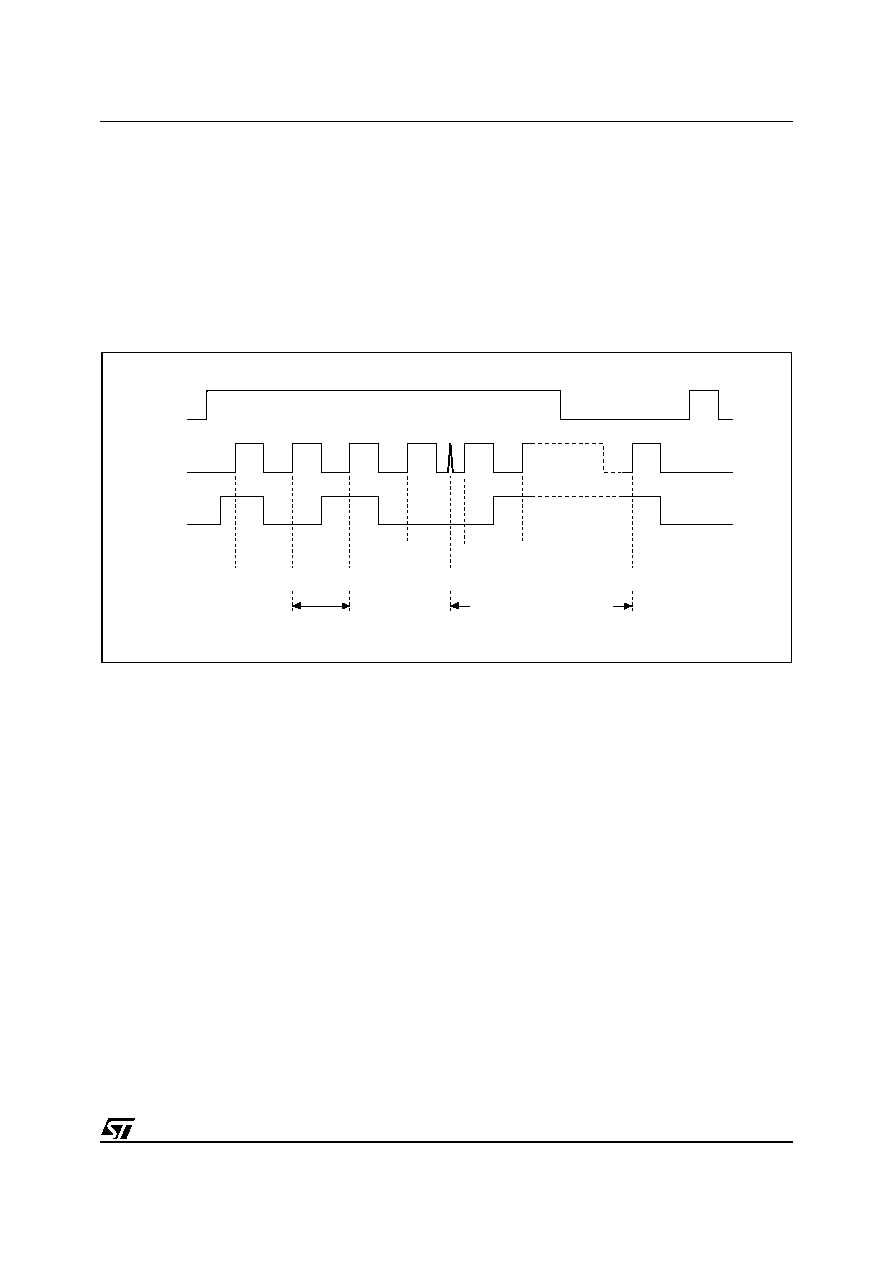
Figure 8. Write Sequence with One Clock Glitch
CLOCK PULSE COUNTER
In a noisy environment, the number of pulses re-
ceived on Serial Clock (C) may be greater than the
number delivered by the Bus Master (the micro-
controller). This can lead to a misalignment of the
instruction of one or more bits (as shown in
Figure
8.
) and may lead to the writing of erroneous data
at an erroneous address.
To combat this problem, the M93Sx6 has an on-
chip counter that counts the clock pulses from the
start bit until the falling edge of the Chip Select In-
put (S). If the number of clock pulses received is
not the number expected, the WRITE, PAWRITE,
WRALL, PRWRITE or PRCLEAR instruction is
aborted, and the contents of the memory are not
modified.
The number of clock cycles expected for each in-
struction, and for each member of the M93Sx6
family, are summarized in
Table 2.
to
Table 3.
. For
example, a Write Data to Memory (WRITE) in-
struction on the M93S56 (or M93S66) expects 27
clock cycles from the start bit to the falling edge of
Chip Select Input (S). That is:
1 Start bit
+ 2 Op-code bits
+ 8 Address bits
+ 16 Data bits
AI01395
S
An-1
C
D
WRITE
START
D0
"1"
"0"
An
Glitch
An-2
ADDRESS AND DATA
ARE SHIFTED BY ONE BIT

M93S66, M93S56, M93S46
16/34
MAXIMUM RATING
Stressing the device above the rating listed in the
Absolute Maximum Ratings" table may cause per-
manent damage to the device. These are stress
ratings only and operation of the device at these or
any other conditions above those indicated in the
Operating sections of this specification is not im-
plied. Exposure to Absolute Maximum Rating con-
ditions for extended periods may affect device
reliability. Refer also to the STMicroelectronics
SURE Program and other relevant quality docu-
ments.
Table 4. Absolute Maximum Ratings
Note: 1. Compliant with JEDEC Std J-STD-020B (for small body, Sn-Pb or Pb assembly), the ST ECOPACK
Æ
7191395 specification, and
the European directive on Restrictions on Hazardous Substances (RoHS) 2002/95/EU
2. JEDEC Std JESD22-A114A (C1=100 pF, R1=1500
, R2=500
)
Symbol
Parameter
Min.
Max.
Unit
T
STG
Storage Temperature
≠65
150
∞C
T
LEAD
Lead Temperature during Soldering
See note
1
∞C
V
OUT
Output range (Q = V
OH
or Hi-Z)
≠0.50
V
CC
+0.5
V
V
IN
Input range
≠0.50
V
CC
+1
V
V
CC
Supply Voltage
≠0.50
6.5
V
V
ESD
Electrostatic Discharge Voltage (Human Body model)
2
≠4000
4000
V

17/34
M93S66, M93S56, M93S46
DC AND AC PARAMETERS
This section summarizes the operating and mea-
surement conditions, and the DC and AC charac-
teristics of the device. The parameters in the DC
and AC Characteristic tables that follow are de-
rived from tests performed under the Measure-
ment Conditions summarized in the relevant
tables. Designers should check that the operating
conditions in their circuit match the measurement
conditions when relying on the quoted parame-
ters.
Table 5. Operating Conditions (M93Sx6)
Table 6. Operating Conditions (M93Sx6-W)
Table 7. Operating Conditions (M93Sx6-R)
Table 8. AC Measurement Conditions (M93Sx6)
Note: Output Hi-Z is defined as the point where data out is no longer driven.
Table 9. AC Measurement Conditions (M93Sx6-W and M93Sx6-R)
Note: Output Hi-Z is defined as the point where data out is no longer driven.
Symbol
Parameter
Min.
Max.
Unit
V
CC
Supply Voltage
4.5
5.5
V
T
A
Ambient Operating Temperature (Device Grade 6)
≠40
85
∞C
Ambient Operating Temperature (Device Grade 3)
≠40
125
∞C
Symbol
Parameter
Min.
Max.
Unit
V
CC
Supply Voltage
2.5
5.5
V
T
A
Ambient Operating Temperature (Device Grade 6)
≠40
85
∞C
Symbol
Parameter
Min.
Max.
Unit
V
CC
Supply Voltage
1.8
5.5
V
T
A
Ambient Operating Temperature (Device Grade 6)
≠40
85
∞C
Symbol
Parameter
Min.
Max.
Unit
C
L
Load Capacitance
100
pF
Input Rise and Fall Times
50
ns
Input Pulse Voltages
0.4 V to 2.4 V
V
Input Timing Reference Voltages
1.0 V and 2.0 V
V
Output Timing Reference Voltages
0.8 V and 2.0 V
V
Symbol
Parameter
Min.
Max.
Unit
C
L
Load Capacitance
100
pF
Input Rise and Fall Times
50
ns
Input Pulse Voltages
0.2V
CC
to 0.8V
CC
V
Input Timing Reference Voltages
0.3V
CC
to 0.7V
CC
V
Output Timing Reference Voltages
0.3V
CC
to 0.7V
CC
V

M93S66, M93S56, M93S46
18/34
Figure 9. AC Testing Input Output Waveforms
Table 10. Capacitance
Note: Sampled only, not 100% tested, at T
A
=25∞C and a frequency of 1 MHz.
Symbol
Parameter
Test Condition
Min
Max
Unit
C
OUT
Output
Capacitance
V
OUT
= 0V
5
pF
C
IN
Input
Capacitance
V
IN
= 0V
5
pF
AI02791
2.4V
0.4V
2.0V
0.8V
2V
1V
INPUT
OUTPUT
0.8VCC
0.2VCC
0.7VCC
0.3VCC
M93SXX-W & M93SXX-R
M93SXX

19/34
M93S66, M93S56, M93S46
Table 11. DC Characteristics (M93Sx6, Device Grade 6)
Note: 1. Current product: identified by Process Identification letter F or M.
2. New product: identified by Process Identification letter W or G.
Table 12. DC Characteristics (M93Sx6, Device Grade 3)
Note: 1. Current product: identified by Process Identification letter F or M.
2. New product: identified by Process Identification letter W or G.
Symbol
Parameter
Test Condition
Min.
Max.
Unit
I
LI
Input Leakage Current
0V
V
IN
V
CC
±2.5
µA
I
LO
Output Leakage Current
0V
V
OUT
V
CC
, Q in Hi-Z
±2.5
µA
I
CC
Supply Current
V
CC
= 5V, S = V
IH
, f = 1 MHz, Current
Product
1
1.5
mA
V
CC
= 5V, S = V
IH
, f = 2 MHz, New
Product
2
2
mA
I
CC1
Supply Current (Stand-by)
V
CC
= 5V, S = V
SS
, C = V
SS
,
Current Product
1
50
µA
V
CC
= 5V, S = V
SS
, C = V
SS
,
New Product
2
15
µA
V
IL
Input Low Voltage
V
CC
= 5V ± 10%
≠0.45
0.8
V
V
IH
Input High Voltage
V
CC
= 5V ± 10%
2
V
CC
+ 1
V
V
OL
Output Low Voltage
V
CC
= 5V, I
OL
= 2.1mA
0.4
V
V
OH
Output High Voltage
V
CC
= 5V, I
OH
= ≠400µA
2.4
V

M93S66, M93S56, M93S46
20/34
Table 13. DC Characteristics (M93Sx6-W, Device Grade 6)
Note: 1. Current product: identified by Process Identification letter F or M.
2. New product: identified by Process Identification letter W or G.
Symbol
Parameter
Test Condition
Min.
Max.
Unit
I
LI
Input Leakage Current
0V
V
IN
V
CC
±2.5
µA
I
LO
Output Leakage Current
0V
V
OUT
V
CC
, Q in Hi-Z
±2.5
µA
I
CC
Supply Current (CMOS
Inputs)
V
CC
= 5V, S = V
IH
, f = 1 MHz, Current
Product
1
1.5
mA
V
CC
= 2.5V, S = V
IH
, f = 1 MHz, Current
Product
1
1
mA
V
CC
= 5V, S = V
IH
, f = 2 MHz, New
Product
2
2
mA
V
CC
= 2.5V, S = V
IH
, f = 2 MHz, New
Product
2
1
mA
I
CC1
Supply Current (Stand-by)
V
CC
= 2.5V, S = V
SS
, C = V
SS
,
Current Product
1
10
µA
V
CC
= 2.5V, S = V
SS
, C = V
SS
,
New Product
2
5
µA
V
IL
Input Low Voltage (D, C, S)
≠0.45
0.2 V
CC
V
V
IH
Input High Voltage (D, C, S)
0.7 V
CC
V
CC
+ 1
V
V
OL
Output Low Voltage (Q)
V
CC
= 5V, I
OL
= 2.1mA
0.4
V
V
CC
= 2.5V, I
OL
= 100µA
0.2
V
V
OH
Output High Voltage (Q)
V
CC
= 5V, I
OH
= ≠400µA
2.4
V
V
CC
= 2.5V, I
OH
= ≠100µA
V
CC
≠0.2
V

21/34
M93S66, M93S56, M93S46
Table 14. DC Characteristics (M93Sx6-W, Device Grade 3)
Note: 1. New product: identified by Process Identification letter W or G.
Table 15. DC Characteristics (M93Sx6-R)
Note: 1. Preliminary Data: this product is under development. For more infomation, please contact your nearest ST sales office.
Symbol
Parameter
Test Condition
Min
1
.
Max.
1
Unit
I
LI
Input Leakage Current
0V
V
IN
V
CC
±2.5
µA
I
LO
Output Leakage Current
0V
V
OUT
V
CC
, Q in Hi-Z
±2.5
µA
I
CC
Supply Current (CMOS
Inputs)
V
CC
= 5V, S = V
IH
, f = 2 MHz
2
mA
V
CC
= 2.5V, S = V
IH
, f = 2 MHz
1
mA
I
CC1
Supply Current (Stand-by)
V
CC
= 2.5V, S = V
SS
, C = V
SS
5
µA
V
IL
Input Low Voltage (D, C, S)
≠0.45
0.2 V
CC
V
V
IH
Input High Voltage (D, C, S)
0.7 V
CC
V
CC
+ 1
V
V
OL
Output Low Voltage (Q)
V
CC
= 5V, I
OL
= 2.1mA
0.4
V
V
CC
= 2.5V, I
OL
= 100µA
0.2
V
V
OH
Output High Voltage (Q)
V
CC
= 5V, I
OH
= ≠400µA
2.4
V
V
CC
= 2.5V, I
OH
= ≠100µA
V
CC
≠0.2
V
Symbol
Parameter
Test Condition
Min.
1
Max.
1
Unit
I
LI
Input Leakage Current
0V
V
IN
V
CC
±2.5
µA
I
LO
Output Leakage Current
0V
V
OUT
V
CC
, Q in Hi-Z
±2.5
µA
I
CC
Supply Current (CMOS
Inputs)
V
CC
= 5V, S = V
IH
, f = 2 MHz
2
mA
V
CC
= 1.8V, S = V
IH
, f = 1 MHz
1
mA
I
CC1
Supply Current (Stand-by)
V
CC
= 1.8V, S = V
SS
, C = V
SS
2
µA
V
IL
Input Low Voltage (D, C, S)
≠0.45
0.2 V
CC
V
V
IH
Input High Voltage (D, C, S)
0.8 V
CC
V
CC
+ 1
V
V
OL
Output Low Voltage (Q)
V
CC
= 1.8V, I
OL
= 100µA
0.2
V
V
OH
Output High Voltage (Q)
V
CC
= 1.8V, I
OH
= ≠100µA
V
CC
≠0.2
V

M93S66, M93S56, M93S46
22/34
Table 16. AC Characteristics (M93Sx6, Device Grade 6 or 3)
Note: 1. t
CHCL
+ t
CLCH
1 / f
C
.
2. Chip Select Input (S) must be brought Low for a minimum of tSLSH between consecutive instruction cycles.
3. Current product: identified by Process Identification letter F or M.
4. New product: identified by Process Identification letter W or G.
Test conditions specified in
Table 8.
and
Table 5.
Symbol
Alt.
Parameter
Min.
3
Max.
3
Min.
4
Max.
4
Unit
f
C
f
SK
Clock Frequency
D.C.
1
D.C.
2
MHz
t
PRVCH
t
PRES
Protect Enable Valid to Clock High
50
50
ns
t
WVCH
t
PES
Write Enable Valid to Clock High
50
50
ns
t
CLPRX
t
PREH
Clock Low to Protect Enable Transition
0
0
ns
t
SLWX
t
PEH
Chip Select Low to Write Enable
Transition
250
250
ns
t
SLCH
Chip Select Low to Clock High
250
50
ns
t
SHCH
t
CSS
Chip Select Set-up Time
M93C46, M93C56, M93C66
50
50
ns
Chip Select Set-up time
M93C76, M93C86
100
50
ns
t
SLSH
2
t
CS
Chip Select Low to Chip Select High
250
200
ns
t
CHCL
1
t
SKH
Clock High Time
250
200
ns
t
CLCH
1
t
SKL
Clock Low Time
250
200
ns
t
DVCH
t
DIS
Data In Set-up Time
100
50
ns
t
CHDX
t
DIH
Data In Hold Time
100
50
ns
t
CLSH
t
SKS
Clock Set-up Time (relative to S)
100
50
ns
t
CLSL
t
CSH
Chip Select Hold Time
0
0
ns
t
SHQV
t
SV
Chip Select to Ready/Busy Status
400
200
ns
t
SLQZ
t
DF
Chip Select Low to Output Hi-Z
200
100
ns
t
CHQL
t
PD0
Delay to Output Low
400
200
ns
t
CHQV
t
PD1
Delay to Output Valid
400
200
ns
t
W
t
WP
Erase/Write Cycle time
10
5
ms

23/34
M93S66, M93S56, M93S46
Table 17. AC Characteristics (M93Sx6-W, Device Grade 6)
Note: 1. t
CHCL
+ t
CLCH
1 / f
C
.
2. Chip Select Input (S) must be brought Low for a minimum of tSLSH between consecutive instruction cycles.
3. Current product: identified by Process Identification letter F or M.
4. New product: identified by Process Identification letter W or G.
Test conditions specified in
Table 9.
and
Table 6.
Symbol
Alt.
Parameter
Min.
3
Max.
3
Min.
4
Max.
4
Unit
f
C
f
SK
Clock Frequency
D.C.
1
D.C.
2
MHz
t
PRVCH
t
PRES
Protect Enable Valid to Clock High
50
50
ns
t
WVCH
t
PES
Write Enable Valid to Clock High
50
50
ns
t
CLPRX
t
PREH
Clock Low to Protect Enable Transition
0
0
ns
t
SLWX
t
PEH
Chip Select Low to Write Enable
Transition
250
250
ns
t
SLCH
Chip Select Low to Clock High
250
50
ns
t
SHCH
t
CSS
Chip Select Set-up Time
100
50
ns
t
SLSH
2
t
CS
Chip Select Low to Chip Select High
1000
200
ns
t
CHCL
1
t
SKH
Clock High Time
350
200
ns
t
CLCH
1
t
SKL
Clock Low Time
250
200
ns
t
DVCH
t
DIS
Data In Set-up Time
100
50
ns
t
CHDX
t
DIH
Data In Hold Time
100
50
ns
t
CLSH
t
SKS
Clock Set-up Time (relative to S)
100
50
ns
t
CLSL
t
CSH
Chip Select Hold Time
0
0
ns
t
SHQV
t
SV
Chip Select to Ready/Busy Status
400
200
ns
t
SLQZ
t
DF
Chip Select Low to Output Hi-Z
200
100
ns
t
CHQL
t
PD0
Delay to Output Low
400
200
ns
t
CHQV
t
PD1
Delay to Output Valid
400
200
ns
t
W
t
WP
Erase/Write Cycle time
10
5
ms

M93S66, M93S56, M93S46
24/34
Table 18. AC Characteristics (M93Sx6-W, Device Grade 3)
Note: 1. t
CHCL
+ t
CLCH
1 / f
C
.
2. Chip Select Input (S) must be brought Low for a minimum of tSLSH between consecutive instruction cycles.
3. New product: identified by Process Identification letter W or G.
Test conditions specified in
Table 9.
and
Table 6.
Symbol
Alt.
Parameter
Min.
3
Max.
3
Unit
f
C
f
SK
Clock Frequency
D.C.
2
MHz
t
PRVCH
t
PRES
Protect Enable Valid to Clock High
50
ns
t
WVCH
t
PES
Write Enable Valid to Clock High
50
ns
t
CLPRX
t
PREH
Clock Low to Protect Enable Transition
0
ns
t
SLWX
t
PEH
Chip Select Low to Write Enable Transition
250
ns
t
SLCH
Chip Select Low to Clock High
50
ns
t
SHCH
t
CSS
Chip Select Set-up Time
50
ns
t
SLSH
2
t
CS
Chip Select Low to Chip Select High
200
ns
t
CHCL
1
t
SKH
Clock High Time
200
ns
t
CLCH
1
t
SKL
Clock Low Time
200
ns
t
DVCH
t
DIS
Data In Set-up Time
50
ns
t
CHDX
t
DIH
Data In Hold Time
50
ns
t
CLSH
t
SKS
Clock Set-up Time (relative to S)
50
ns
t
CLSL
t
CSH
Chip Select Hold Time
0
ns
t
SHQV
t
SV
Chip Select to Ready/Busy Status
200
ns
t
SLQZ
t
DF
Chip Select Low to Output Hi-Z
100
ns
t
CHQL
t
PD0
Delay to Output Low
200
ns
t
CHQV
t
PD1
Delay to Output Valid
200
ns
t
W
t
WP
Erase/Write Cycle time
5
ms

25/34
M93S66, M93S56, M93S46
Table 19. AC Characteristics (M93Sx6-R)
Note: 1. t
CHCL
+ t
CLCH
1 / f
C
.
2. Chip Select Input (S) must be brought Low for a minimum of tSLSH between consecutive instruction cycles.
3. Preliminary Data: this product is under development. For more infomation, please contact your nearest ST sales office.
Test conditions specified in
Table 9.
and
Table 7.
Symbol
Alt.
Parameter
Min.
3
Max.
3
Unit
f
C
f
SK
Clock Frequency
D.C.
1
MHz
t
PRVCH
t
PRES
Protect Enable Valid to Clock High
50
ns
t
WVCH
t
PES
Write Enable Valid to Clock High
50
ns
t
CLPRX
t
PREH
Clock Low to Protect Enable Transition
0
ns
t
SLWX
t
PEH
Chip Select Low to Write Enable Transition
250
ns
t
SLCH
Chip Select Low to Clock High
250
ns
t
SHCH
t
CSS
Chip Select Set-up Time
50
ns
t
SLSH
2
t
CS
Chip Select Low to Chip Select High
250
ns
t
CHCL
1
t
SKH
Clock High Time
250
ns
t
CLCH
1
t
SKL
Clock Low Time
250
ns
t
DVCH
t
DIS
Data In Set-up Time
100
ns
t
CHDX
t
DIH
Data In Hold Time
100
ns
t
CLSH
t
SKS
Clock Set-up Time (relative to S)
100
ns
t
CLSL
t
CSH
Chip Select Hold Time
0
ns
t
SHQV
t
SV
Chip Select to Ready/Busy Status
400
ns
t
SLQZ
t
DF
Chip Select Low to Output Hi-Z
200
ns
t
CHQL
t
PD0
Delay to Output Low
400
ns
t
CHQV
t
PD1
Delay to Output Valid
400
ns
t
W
t
WP
Erase/Write Cycle time
10
ms

M93S66, M93S56, M93S46
26/34
Figure 10. Synchronous Timing (Start and Op-Code Input)
Figure 11. Synchronous Timing (Read or Write)
PRE
W
C
S
D
OP CODE
OP CODE
START
START
OP CODE INPUT
tCHDX
tDVCH
tCLSH
tCLCH
tCHCL
tWVCH
tPRVCH
AI02025
tSHCH
AI002026
C
D
Q
ADDRESS INPUT
Hi-Z
tDVCH
tCLSL
A0
S
DATA OUTPUT
tCHQV
tCHDX
tCHQL
An
tSLSH
tSLQZ
Q15
Q0

27/34
M93S66, M93S56, M93S46
Figure 12. Synchronous Timing (Read or Write)
PRE
W
C
S
D
Hi-Z
tW
tDVCH
AI02027
Q
tCLPRX
tSLWX
tCLSL
tCHDX
tSLSH
tSLQZ
BUSY
tSHQV
READY
WRITE CYCLE
ADDRESS/DATA INPUT
An
A0/D0
tSLCH

M93S66, M93S56, M93S46
28/34
PACKAGE MECHANICAL
Figure 13. PDIP8 ≠ 8 pin Plastic DIP, 0.25mm lead frame, Package Outline
Note: Drawing is not to scale.
Table 20. PDIP8 ≠ 8 pin Plastic DIP, 0.25mm lead frame, Package Mechanical Data
Symb.
mm
inches
Typ.
Min.
Max.
Typ.
Min.
Max.
A
5.33
0.210
A1
0.38
0.015
A2
3.30
2.92
4.95
0.130
0.115
0.195
b
0.46
0.36
0.56
0.018
0.014
0.022
b2
1.52
1.14
1.78
0.060
0.045
0.070
c
0.25
0.20
0.36
0.010
0.008
0.014
D
9.27
9.02
10.16
0.365
0.355
0.400
E
7.87
7.62
8.26
0.310
0.300
0.325
E1
6.35
6.10
7.11
0.250
0.240
0.280
e
2.54
≠
≠
0.100
≠
≠
eA
7.62
≠
≠
0.300
≠
≠
eB
10.92
0.430
L
3.30
2.92
3.81
0.130
0.115
0.150
PDIP-B
A2
A1
A
L
b
e
D
E1
8
1
c
eA
b2
eB
E

29/34
M93S66, M93S56, M93S46
Figure 14. SO8 narrow ≠ 8 lead Plastic Small Outline, 150 mils body width, Package Outline
Note: Drawing is not to scale.
Table 21. SO8 narrow ≠ 8 lead Plastic Small Outline, 150 mils body width, Package Mechanical Data
Symb.
mm
inches
Typ.
Min.
Max.
Typ.
Min.
Max.
A
1.35
1.75
0.053
0.069
A1
0.10
0.25
0.004
0.010
B
0.33
0.51
0.013
0.020
C
0.19
0.25
0.007
0.010
D
4.80
5.00
0.189
0.197
E
3.80
4.00
0.150
0.157
e
1.27
≠
≠
0.050
≠
≠
H
5.80
6.20
0.228
0.244
h
0.25
0.50
0.010
0.020
L
0.40
0.90
0.016
0.035
0∞
8∞
0∞
8∞
N
8
8
CP
0.10
0.004
SO-a
E
N
CP
B
e
A
D
C
L
A1
1
H
h x 45∞

M93S66, M93S56, M93S46
30/34
Figure 15. TSSOP8 3x3mm≤ ≠ 8 lead Thin Shrink Small Outline, 3x3mm≤ body size, Package Outline
Note: Drawing is not to scale.
Table 22. TSSOP8 3x3mm≤ ≠ 8 lead Thin Shrink Small Outline, 3x3mm≤ body size, Mechanical Data
Symbol
mm
inches
Typ.
Min.
Max.
Typ.
Min.
Max.
A
1.100
0.0433
A1
0.050
0.150
0.0020
0.0059
A2
0.850
0.750
0.950
0.0335
0.0295
0.0374
b
0.250
0.400
0.0098
0.0157
c
0.130
0.230
0.0051
0.0091
D
3.000
2.900
3.100
0.1181
0.1142
0.1220
E
4.900
4.650
5.150
0.1929
0.1831
0.2028
E1
3.000
2.900
3.100
0.1181
0.1142
0.1220
e
0.650
≠
≠
0.0256
≠
≠
CP
0.100
0.0039
L
0.550
0.400
0.700
0.0217
0.0157
0.0276
L1
0.950
0.0374
0∞
6∞
0∞
6∞
TSSOP8BM
1
8
CP
c
L
E
E1
D
A2
A
e
b
4
5
A1
L1

31/34
M93S66, M93S56, M93S46
Figure 16. TSSOP8 ≠ 8 lead Thin Shrink Small Outline, Package Outline
Note: Drawing is not to scale.
Table 23. TSSOP8 ≠ 8 lead Thin Shrink Small Outline, Package Mechanical Data
Symbol
mm
inches
Typ.
Min.
Max.
Typ.
Min.
Max.
A
1.200
0.0472
A1
0.050
0.150
0.0020
0.0059
A2
1.000
0.800
1.050
0.0394
0.0315
0.0413
b
0.190
0.300
0.0075
0.0118
c
0.090
0.200
0.0035
0.0079
CP
0.100
0.0039
D
3.000
2.900
3.100
0.1181
0.1142
0.1220
e
0.650
≠
≠
0.0256
≠
≠
E
6.400
6.200
6.600
0.2520
0.2441
0.2598
E1
4.400
4.300
4.500
0.1732
0.1693
0.1772
L
0.600
0.450
0.750
0.0236
0.0177
0.0295
L1
1.000
0.0394
0∞
8∞
0∞
8∞
TSSOP8AM
1
8
CP
c
L
E
E1
D
A2
A
e
b
4
5
A1
L1

M93S66, M93S56, M93S46
32/34
PART NUMBERING
Table 24. Ordering Information Scheme
Note: 1. ST strongly recommends the use of the Automotive Grade devices for use in an automotive environment. The High Reliability Cer-
tified Flow (HRCF) is described in the quality note QNEE9801. Please ask your nearest ST sales office for a copy.
2. Available only on new products: identified by the Process Identification letter W or G.
Devices are shipped from the factory with the
memory content set at all 1s (FFh).
For a list of available options (speed, package,
etc.) or for further information on any aspect of this
device, please contact your nearest ST Sales Of-
fice.
Table 25. How to Identify Current and New Products by the Process Identification Letter
Note: 1. This example comes from the S08 package. Other packages have similar information. For further information, please ask your ST
Sales Office for Process Change Notice PCN MPG/EE/0059 (PCEE0059).
Example:
M93S66
≠
W MN
6
T
P
Device Type
M93 = MICROWIRE serial access EEPROM (x16) with
Block Protection
Device Function
66 = 4 Kbit (256 x 16)
56 = 2 Kbit (128 x 16)
46 = 1 Kbit (64 x 16)
Operating Voltage
blank = V
CC
= 4.5 to 5.5V
W = V
CC
= 2.5 to 5.5V
R = V
CC
= 1.8 to 5.5V
Package
BN = PDIP8
MN = SO8 (150 mil width)
DW = TSSOP8 (169 mil width)
DS
2
= TSSOP8 (3x3mm body size)
Device Grade
6 = Industrial: device tested with standard test flow over ≠40 to 85 ∞C
3 = Automotive: device tested with High Reliability Certified Flow
1
over ≠40 to 125 ∞C
Option
blank = Standard Packing
T = Tape & Reel Packing
Plating Technology
blank = Standard SnPb plating
P = Lead-Free and RoHS compliant
G = Lead-Free, RoHS compliant, Sb
2
O
3
-free and TBBA-free
Markings on Current Products
1
Markings on New Products
1
M93S46W6
AYWWF (or AYWWM)
M93S46W6
AYWWW (or AYWWG)

33/34
M93S66, M93S56, M93S46
REVISION HISTORY
Table 26. Document Revision History
Date
Rev.
Description of Revision
07-Mar-2002
2.0
Document reformatted, and reworded, using the new template. Temperature range 1 removed.
TSSOP8 (3x3mm) package added. New products, identified by the process letter W, added,
with fc(max) increased to 1MHz for -R voltage range, and to 2MHz for all other ranges (and
corresponding parameters adjusted).
26-Mar-2003
2.1
Value of standby current (max) corrected in DC characteristics tables for -W and -R ranges
V
OUT
and V
IN
separated from V
IO
in the Absolute Maximum Ratings table
14-Apr-2003
2.2
Values corrected in AC characteristics tables for -W range (tSLSH, tDVCH, tCLSL) for devices
with Process Identification Letter W.
23-May-2003
2.3
Standby current corrected for -R range. Four missing parameters restored to all AC
Characteristics tables
24-Nov-2003
3.0
Table of contents, and Pb-free options added. V
IL
(min) improved to -0.45V.
19-Apr-2004
4.0
Absolute Maximum Ratings for V
IO
(min) and V
CC
(min) changed. Soldering temperature
information clarified for RoHS compliant devices. Device Grade 3 clarified, with reference to
HRCF and automotive environments. Process identification letter "G" information added

M93S66, M93S56, M93S46
34/34
Information furnished is believed to be accurate and reliable. However, STMicroelectronics assumes no responsibility for the consequences
of use of such information nor for any infringement of patents or other rights of third parties which may result from its use. No license is granted
by implication or otherwise under any patent or patent rights of STMicroelectronics. Specifications mentioned in this publication are subject
to change without notice. This publication supersedes and replaces all information previously supplied. STMicroelectronics products are not
authorized for use as critical components in life support devices or systems without express written approval of STMicroelectronics.
The ST logo is a registered trademark of STMicroelectronics.
All other names are the property of their respective owners.
© 2004 STMicroelectronics - All rights reserved
STMicroelectronics GROUP OF COMPANIES
Australia - Belgium - Brazil - Canada - China - Czech Republic - Finland - France - Germany -
Hong Kong - India - Israel - Italy - Japan - Malaysia - Malta - Morocco - Singapore -
Spain - Sweden - Switzerland - United Kingdom - United States
www.st.com